INA209 Hardware description
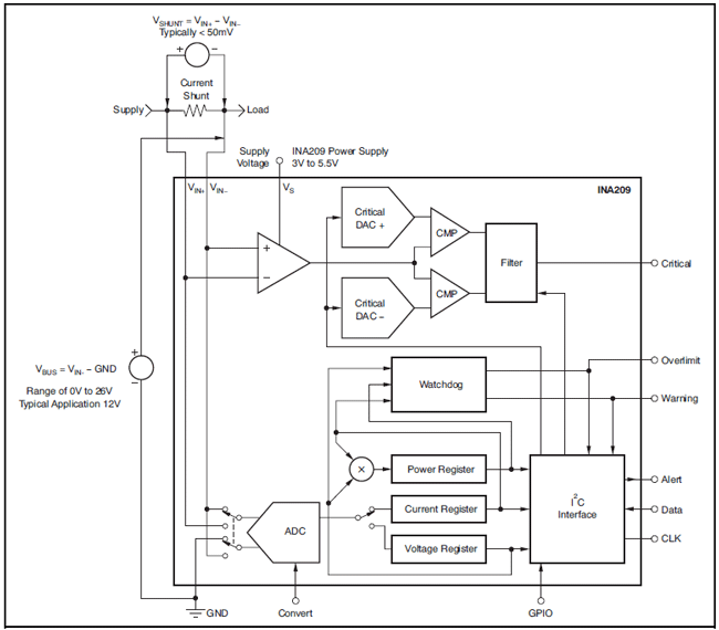
The INA209 is a high-side current shunt and power monitor with an I2C interface. The INA209 monitors both shunt drop and shunt bus voltage. A programmable calibration value, combined with an internal multiplier, enables direct readouts in amperes. An additional multiplying register calculates power in watts. The INA209 features two separate, onboard watchdog capabilities: a warning comparator and an over-limit comparator. The warning comparator is useful for monitoring lower warning limits and incorporates a user-defined delay. The over-limit comparator assists with monitoring upper limits that could require immediate system shutdown.
The INA209 also includes an analog comparator and a programmable digital-to-analog converter (DAC) that combine to provide the fastest possible responses to current overload conditions. The INA209 can be used together with hot swap controllers that already use a current sense resistor. The INA209 full-scale range can be selected to be either within the hot-swap controller sense limits, or wide enough to include them.
The INA209 senses across shunts on buses that can vary from 0V to 26V. The device uses a single +3V to +5.5V supply, drawing a maximum of 1.5mA of supply current. It is specified for operation from –25°C to +85°C.
Features
- Senses BUS Voltage from 0V to +26V
- Reports Current, Voltage, Power and stores Peaks
- Triple Watchdog Limit:
- Lower Warning with Delay
- Upper Over-Limit, No Delay
- Fast Analog Critical
- High Accuracy: 1% Max Over Temp
Application
Servers, Telecom Equipment, Automotive, Power Management, Battery Chargers, Welding Equipment, Power Supplies, Test Equipment.
Absolute Maximum Ratings

(1) Stresses above these ratings may cause permanent damage. Exposure to absolute maximum conditions for extended periods may degrade device reliability. These are stress ratings only, and functional operation of the device at these or any other conditions beyond those specified is not implied.
(2) VIN+ and VIN– may have a differential voltage of –26V to +26V; however, the voltage at these pins must not exceed the range –0.3V to +26V
Electrical Characteristics at Vs=+3.3V
Boldface limits apply over the specified temperature range, TA = –25°C to +85°C.
At TA = +25°C, VIN+ = 12V, VSENSE = (VIN+ – VIN–) = 32mV, PGA = ÷ 1, and BRNG(1) = 1, unless otherwise noted.

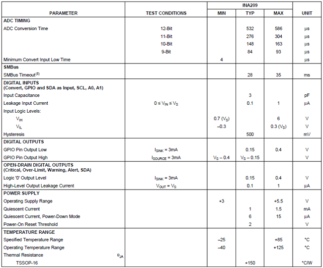
(1) BRNG is bit 13 of the Configuration Register.
(2) This parameter only expresses the full-scale range of the ADC scaling. In no event should more than 26V be applied to this device.
(3) Referred-to-input (RTI).
(4) User-programmable. See the Critical Comparator and Register sections.
(5) SMBus timeout in the INA209 resets the interface any time SCL or SDA is low for over 28ms.
PIN Configuration
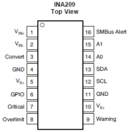
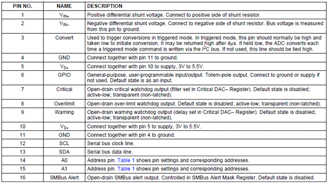
PIN Description
Tipical Application Circuit
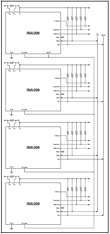
Multichannel Data Acquisition with Simultaneous Sampling
The INA209 can be used in multiple current measurement channels where the controlling processor sums the currents of all the channels for a total current. Often these current measurements must occur simultaneously. Use the GPIO output from one of the INA209s and connect it to the Convert pin of the other INA209s.
Software Library Description
The INA209 Arduino Library use the Arduino Wire Library for I2C communication. For I2C communication, Arduino works as a Master device and the INA209 works as a Slave device.
The INA209 has two address pins, A0 and A1. Table 1 describes the pin logic levels for each of the 16 possible addresses. First of all you have to set the slave address by connecting A0 and A1 pins as specified in the table below.
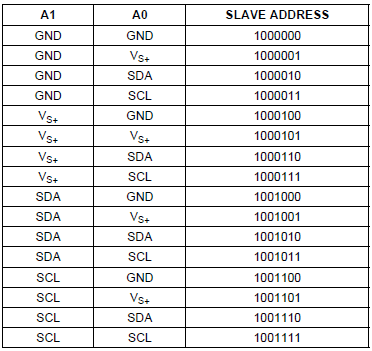
Table1 - Slave Adress
This is the electrical connections, I have used an Arduino UNO and an INA209:
INA209 PIN 1 (Vin+) to positive side of 0,1 Ohm shunt resistor
INA209 PIN 2 (Vin-) to negative side of 0,1 Ohm shunt resistor
INA209 PIN 4 (GND) to power supply ground
INA209 PIN 5 (Vs+) to power supply 3V to 5,5V
INA209 PIN 10 (Vs+) to power supply 3V to 5,5V
INA209 PIN 11 (GND) to power supply ground
INA209 PIN 12 (SCL) ANALOG PIN 5 for ARDUINO UNO
INA209 PIN 13 (SDA) ANALOG PIN 4 for ARDUINO UNO
INA209 PIN 14 (A0) to power supply ground for set slave address to 0x40 (example)
INA209 PIN 15 (A1) to power supply ground for set slave address to 0x40 (example)
Download the library files.
For use the INA209 library you have to copy the entire INA209 directory with INA209.h and INA209.cpp files in the Arduino "/libraries" directory.
Now you can start Arduino software (I have used ver. 1.0.1) and create a new sketch.
Add this in your sketch:
When you create an istance of the INA209 class you have to set the slave address that you have setted by A0 and A1 pins of INA209 chip.
Start I2C BUS communication and set Arduino as a Master device with Wire.begin(); as follow:
Now you have to write the General Configuration Register. You have to see the datasheet.
For example if you want this parameters:
Bus Voltage Range = 32V
PGA (Shunt Voltage Only) = +/- 320mV
BADC Bus ADC Resolution/Averaging = 12bit
SADC Shunt ADC Resolution/Averaging = 12bit
Operating Mode = Shunt and Bus, Continuos
You have to write the decimal value of 14751 = 11100110011111 bin = 399F hex
If you want the current and power direct reading you have to calculate the calibration value and write the Calibration Register (see the datasheet).
For example:
Vbus_max = 32V
Vshunt_max = 0,32V
Rshunt = 0,1 Ohm
-> Max Expected Current = +/- 3A
Current LSB = 100uA
Calibration Reg = 4096
Power LSB = 2mW
Mas Power = 102,4W
You can set the warnig limit that trigger flags in the Status Register and activate the Warning pin (see the datasheet).
For example you can set:
You can set the over-limit and critical DAC limits that trigger flags to be set in the Status Register and activate the Overlimit pin or the Critical pin (see the datasheet).
Now you can read all the INA209 registers and see the values:
Bibliography
Texas Instruments INA209 Datasheet - High-Side Measurement, Bi-Directional Current/Power Monitor with I2C Interface (Rev. B) (PDF , 1491 KB) 27 Mar 2009 - http://www.ti.com/lit/ds/symlink/ina209.pdf - Some information, material and related graphics ("Materials") available on this pageare provided by Texas Instruments Incorporated web site. This Materials are only for informational use.